
The Saint-Anne's High School's pupils participation to "Jeunes ambassadeurs en CorÚe du Sud"
The Saint-Anne's High School's pupils participation to "Jeunes ambassadeurs en CorÚe du Sud"

_____
We are the Monday 14 July 2025
> Nanotubes

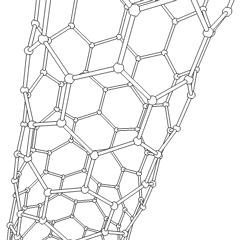
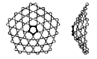
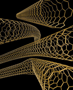
A carbon nanotube
The nanotubes were discovered in 1991 by Sumio Iijima. A carbon nanotube is a tube whose diameter lies between 1 and 10 nanometers. They are a form of structure crystalline of carbon and made up of atoms laid out regularly in pentagons, hexagons or heptagons. They are one of the first industrial products of the field of the nanotechnologies.
The nanotubes are interesting by the principal following characteristics:
The nanotubes of carbon should be approximately 200 times more resistant than steel for a weight 6 times less. The carbon nanotube present a great elasticity and a great flexibility.

The carbon nanotubes are superconductive at low temperature. The carbon nanotubes have also semiconductor properties: they can be insulating or metal according to the electric field in which they are.
The nanotubes are hollow structures, which one can fill with others chemical compounds, so they are closed containers on a nanometer scale, called nanofils. For example, we can fill nanotubes of hydrogen atoms, usefull to store this gas securitly in hydrogen working cars. Then the warm weaken the links holding hydrogene in its carbon cage. ThatÆs the way the combustible is liberated.
In the natural state, carbon exists in a solid state in two crystalline forms, graphite and diamond. Initially we will be interested in these two carbonaceous structures :
If you take a plan of this graphite, called graphene and you roll up it on itself, you obtain a nanotube. The nanotubes can be made of only one graphene, we call them nanotubes monofeuillet or of several graphene then they are called nanotubes multifeuillets. According to the way graphene is folded up, the properties of the nanotube are different. The angle of wrap, also called helicity, determines its electronic properties.
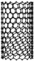
Monofeuillet nanotube
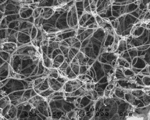
Interlacing of monotubes
The rolling up consists in stacking two hexagons of a graphene wall. The choice of these two hexagons specifies the diameter of the nanotubes and its helicity (T). The angle T varies from 0 to 30 degrees because of the symmetry of the hexagonal network. So it is possible to classify the carbon nanotubes into different families, the chiral and non chiral nanotubes. The hexagons of the upper part of the non chiral nanotubes have the same orientation than the hexagons of the lower part. If the angle T is worth 0 degree, we have a ôzig-zag tubeö. If the angle T is worth 30 degrees, we have an ôarmchair tubeö. The chiral tube forms an Archimedes screw.

Chair tube
Zig zag tube
Chiral tube

Archimede's live
The carbon nanotube is formed by a grapheme wall. We have a tube which is open at its ends so we have to close it. For that, we must insert some flaws of curve in the grapheme plan. There, it is a pentagon. In accordance with the mathematical laws of Euler, 12 pentagons are necessary at least to close the tube.

Ends of nanotubes
Only synthesis nanotubes have been observed at this moment. Since the discovery of these nanotubes, different techniques have been explored. Two ways of synthesis emerged from these techniques. They are different because of the temperature which is used during the synthesis.
With a high temperature, the carbon is evaporated then condensed in a place where there is a high temperature and a partial pressure of an inert gas as helium.
With medium temperature, the graphitisation quality is worse than with a high temperature, but the diameter and the length are more uniform and this is an advantage.
A nanotube is nearly 100.000 times finer than a hair. The traditional optical microscopes, which allows to see dust or bacteria, are not enough powerful to see them. The wavelength of the light, being 400 to 800 nanometers, is too large to observe an object of less than ten nanometers wide.
There are two different microscope able to give indications of the nanotubes :
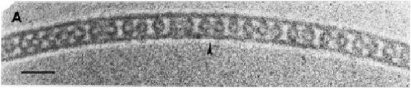
the sweeping electronic microscope, in which an electron beam interacts with the atoms of the molecules that we observe, which allows to recover informations from these molecules. This technique doesnÆt allows to distinguish the atoms one by one, but it is very effective to recognize the nanotubes. We indeed distinctly see the edges of these filaments, or their section. We can even count the number of layers of each nanotube.
the microscope with tunnel effect, offers images of the surface of the nanotubes and makes it possible to distinguish the atoms from the layer external of the nanotube.

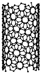
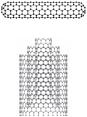
The surface of a nanotube monofeuillet obtained by microscopy with tunnel effect

Principe:
We place a conducting point above the surface of the nanotube. Some free electrons of metal are a bit attracted out of the surface, and if we move the point closer, we can record an electrical current. Thus we measure the current resulting from the passage of electrons between the point and the surface. This current depends on the distance separating the point from surface. Thus, we move the point abov the nanotube with a sweeping motion and we adjust its height to preserve a constant current intensity. We can then determine the profile of the surface.
The fact of being able to observe the nanotubes made it possible to better identify and study them.
Because of its remarkable properties, many applications were found :
The nanotubes have at the same time the adequate size and the ideal electrical properties to replace the current electronic devices :the conducting nanotubes would replace copper wires, while the semiconductors would form functional and logical components with performances higher than silicon.One could thus produce field-effect transistors made up of only one carbon monofeuillet nanotube, then lay out on the same integrated circuit and therefore increase considerably the power of the chips used in the portable computers and mobiles phones.

A Nanotransistor
The nanotubes could thus be used for luminescent lamps, like cold cathode,as portable sources of x-rays with low fuel consumption . the Samsung company from Korea produced devices comprising of a cathode of carbone nanotubes and a phosphorescent screen, able to emit in the visible spectrum with an excellent brightness. These devices consume very little energy and are of a competitive manufacturing cost. It is the first industrial application using carbone nanotubes.
Up to now, flat screens (mainly laptop ones) generally used the liquid crystal technology. The trouble, with liquid crystals, is that they offer colours which lack brightness. However, nanotubes could make it possible to improve this fault of flat screens and would make it rather cheap as well . indeed the nanotubes, perfectly aligned, would be transformed into far more effective transmitters of electrons as they are good electric conductive and concentrate the current on very small surfaces. The difficulty in directing tens of thousands of nanotubes in the same direction remains, not being completely solved for the time being.

Samsung's flat screen
One research actually in process studies the possibility of replacing the filament of the bulb, normally made out of tungsten, by a nanoribbon. At equal temperature, the filament out of nanotubes would have an apparent brightness higher than that out of tungsten, because in addition to the light emission due to the black body effect a luminescence effect is added. However, marketing of these bulbs is not considered before 2010.
Nanotubes bring a mass memory: the nanoRAM. The idea to carry out magnetic wires of nanoscopic size to store information is essential when one considers the appetite of our society for storage. Standard supports of storage of information - hard drive, floppy-disks, SyQuest cartridges - are mainly magnetic. To increase the density of their memory, it is necessary to increase the number of bits per square micron, hence the interest for the smallest possible devices. Each bit is a orientated magnetized element: if the South Pole of magnetization is in top and the North Pole in bottom, in the binary language it means ôyesö, and the opposite ônoö. Once written, information must remain unchanged, in particular during the reading, that is to say that magnetization must preserve its axis - what the thread-like nature of the nanofibres considered help.

Until now, atomic force microscopes (AFM) tips were generally made of silicon or silicon nitride. They are likely to be damaged in contact with surfaces, and the carbon nanotubes could be an alternative, thanks to their great rigidity and their nanometric diameter. It would then be enough to stick a nanotube on an atomic force microscope tip.
Nanotubes, thanks to the large smoothness of their ends, make ideal tips for surface microscopies (tunnel microscopy, with atomic force). They make it possible to improve considerably the resolution of these instruments because the image resolution depends on the radius of curvature on the tip.

Thanks to the resistance to extreme temperatures reached at the time of the passage in atmosphere.

A ribbon of nanotubes will be wedged between the panes of a car, and by powering it, it will de-ice them.
The idea here is to couple an electric request with a mechanical deformation of the object and the nanotube seems to be an object completely adapted for that.
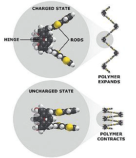
An artificial muscle: The arms and hinges of the polymer are pushed back or attracted to each other respectively when an electric charge is applied and withdrawn, causing the extension and the contraction of the artificial muscle.
Nanotubes, because they are tiny and entirely made out of carbon, are biocompatible, a property which highly interests doctors and biologists. Researchers showed the potential of the nanotubes as electrodes allowing studying directly in the human body, such as for example the oxidation of the dopamine, a neuro-transmitter. Nanotubes could be also used to transport biological materials (drugs). Carbon nanoparticules were finally used by American researchers as microprojectiles nicely called ôbiolositicö to introduce DNA into living cells. One could thus thanks to the nanotubes get rid of cancerous metastases, dissolve clots of blood, improve deteriorated blood circulations (by slackening oxygen at constant rate in blood flow or release on need).
Nanotubes are hollow structures, which one can fill with others chemical compounds. Nanotubes would then be used as closed containers on a nanometric scale - nanowires- to store or protect fragile objects in a hostile environment.
The experiments of filling presented on the figure below prove the feasibility of such applications in particular in organic chemistry.
So many applications tend to make one dream, but a majority of them are for the moment only tested in laboratory, and for some stay only science fiction for now.
After a short reminder of nanotubes and their use in the world, this is now the most important part, what has been done in Korea about nanotechnologies! Which new process have been invented in Korea ?
Actually, South Korean scientists continue to make breakthroughs in potential-laden carbon nanotube, which is called a dream material of the future.

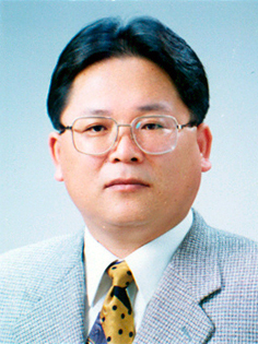
 Ahn Sang-jung
A team of Korean scientists has found the ideal technology to handle the carbon nanotube. The team is led by Ahn Sang-jung at Korea Research Institute of Standards and Science (KRISS), and composed of Inha University and Nanofocus Research InstituteÆs members (Seoul).
How did they succed in ?AhnÆs team accidentally discovered this long-awaited technique in vacuum, using a focused ion beam.
They handle carbon nanotubes in the three dimensional world and applied it to a probe of an AFM. The newly discovered technology of bending carbon nanotubes will accelerate its applications in such segments as field emission display and equipment to gauge semiconductors characteristics.

 Kim Kwang-soo
A team of scientists developed the thinnest carbon nanotubes ever, as slim as 0.4 nanometers in diameter.The team, headed by Prof. Kim Kwang-soo at Pohang University of Science and Technology in Korea, extracted the world's first sub-nanometer carbon tube. Thus far, the thickness of the slimmest carbon nanotube was just over 1 nanometer. This team broke through the barrier using a new idea.

The would-be star substances are categorized into two main types of Carbon and multi-walled ones, which are composed of many single-walled shells. The 0.4-nanometers nanotubes are single-walled. KimÆs team obtained the ultra-thin nanotubes simply by pulling them apart from the multi-walled ones. It is like peeling onions ! They used a needle tip of an atomic force microscope to get rid of many outer layers of a multi-walled nanotube to gain the innermost one, a super-slim single-walled nanotube.
What else ?In addition, KimÆs team reeled out the thin nanotubes to very long distances, 1 millimeter. It is about 1,000 times longer than the previous length of 1 micrometer. They also confirmed the hypothesis that sub-nanometer nanotubes will be metallic rather than being semi-conductive. With their findings, they will be able to open up a new era in the study of nanotubes in full swing.

A team from Sungkyunkwan University, led by professor Lee Young-hee, have invented a new way to harvest semiconducting nanotubes from metallic ones. LeeÆs team said they will open the untapped market of carbon nanotube semiconductors for terabit computers However, the attempts to apply the material to semiconductors have faced setbacks because the technology was not established of separating semiconducting nanotubes from metallic ones. This newfound technology will help overcome the limitation of the current silicon semiconductors around 2015 when nanotech goes main stream in full swing.

Other researchers, led by Seoul National University professor Park Wan-jun, invented a new process to crank out high-purity single-walled carbon nanotubes. Contrary to conventional methods of creating the promising substances at ultra-high temperatures ranging from 700 to 2,000 degrees Celsius, the team was successful at room temperature.
Sum up : In sum up to this part, itÆs important to notice that, in 2010, carbon nanotubes prize is expected to decrease by 10 to 100, and nanotubes global market will break through the 3 billions dollars. And of course, even if Korea is only the 4th global power nowadays, it is expected to be the largest supplier of all types of nanotubes. ItÆs also necessary to precise that, on the 20 companies in the world producing carbon nanotubes in commercial quantity, itÆs Korea which has taken out the most patents. Actually, itÆs the Korean company Samsung which come first with 23 patents on 257.
A memory is always made in the same way: it is composed of a very thin grate of interlaced threads. In each intersection, a bit of information is stocked, 0 or 1 according to the electronic potential which is used.
NRAM or NanoRAM is a new type of electronic memory based on utilisation of carbon nanotubes. In the NanoRAM, the position of the nanotubes from each other (up or low) makes stocking bits possible. We will be able to move a cube to change its ôvalueö.
If so, the position of these tubes stays stable, even if there is no electric current, contrary to present memories (DRAM for example).
The functioning of this memory, NRAM, will necessitate several hundred billions of nanotubes, which have to be organised in regular structures.
NanoRAM could create very fast micro-chips, which can stock until 10 Go of data.
2006, All rights reserved. Design et contents made by lycÚe Saint-Anne of Brest's second students